Above is the finish PCB design that I send for fabrication this afternoon, will post the PCB photo once I got my PCB back from China, hopefully by next week.
First, you need to download the kicad for window, I use this version from:
http://kicad.nosoftware.cz/
The latest build I can find on net is default stable version is 2013, which does not have the latest interactive routing. I wish they could update the stable version to late 2014 build..
Just download from the latest version. I found it to be really stable, no crash so far (after I fix the really annoying PCB footprint library)
Once you install kicad on window, you should copy the PCB footprint library to local disk, default is getting the library from github, which is really slow, and some time cause crash (I think someone fix the github path crash issues, it use to point to some path that is no longer exist).
There is python script that will download all the github library to local disk. But the posted version seem to be have error in it, will post my version later. You can read about the frustration of using the footprint library here.
Basically, you need to download all the footprint library to local disk, here is the step
- Download library using git from python script. (script to be send out later, make sure you install git and python in your PC)
- Copy fp-lib-table.for-pretty from C:\KiCad\share\template to C:\Users\<user>\AppData\Roaming\kicad as fp-lib-table
- create or update runkicad.bat with KISYSMOD to local disk. SET KISYSMOD=C:\kicadlib\kicad\share\github-repo <your local area>
Now you need to start kicad with the bat file, so that it will point to the local library.
Kicad schematic editing is really easy, just open a new project start creating. Here is example of my drone schematic.
Just place and round the schematic, and sometime you may need to design your schematic symbol, which also very easy in kicad. the library editor is really easy to use too, just open an existing symbol, make change and save as your new symbol.
Once you are done with schematic design, the next stage is to create netlist for PCB as well as assigning footprint, it done using another tool call CvPCB.
Once you are done with footprint assignment, you move to PCB design. We base our board design base on MinnowBoard Max lure. you can import the board outline easily, and the Minnowvoard Max board design file is freely downloadable. (pointer to be update later)
Before start editing in PCB, you need to set few more thing, one is the PCB design rule, you need to review you PCB manufacture design rule and update you kicad design rules accordingly. Normally they display the rule at front of the order page, here is the example PCB rule found on ebay:
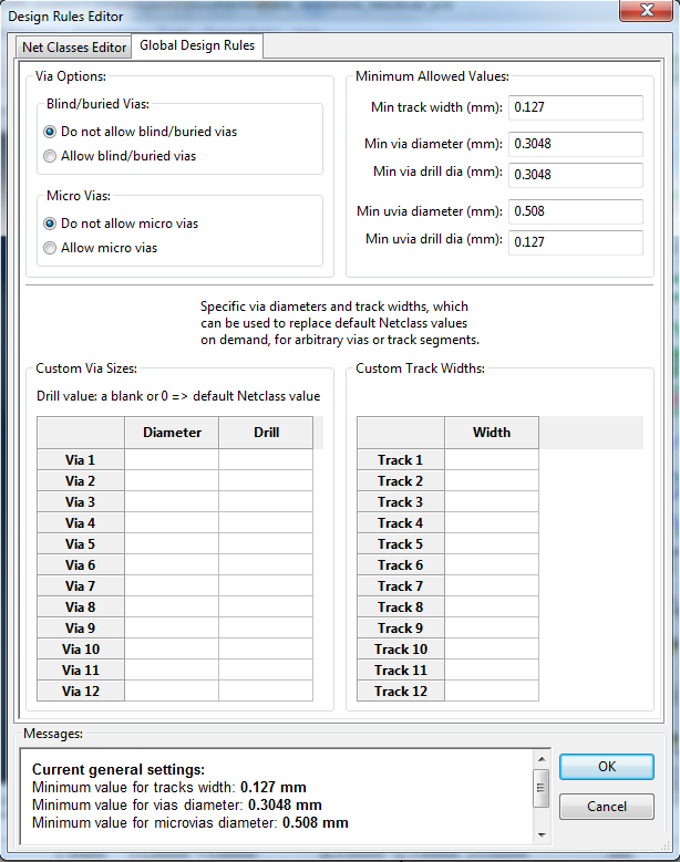
Here is where you set the rule in kicad (Design Rules --> Global Design Rules):
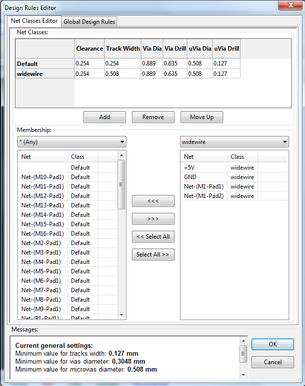
Also you may want to create wide wire for power or some net that need wide track, it better to do this before starting routing, else you need to use "change segment/track width" canvas pulldown menu to change the wire width.
To create wide wire, go to Design Rules --> Net Class Editor. First by adding a new net classes in the window, then select the newly create net class in the pull down menu on the right of membership. You just add and remove the net from the net class.
OK. Once you are done with the design, you need to generate and send the gerber to PCB manufacture for review and quote. Normally they will comeback with some request if there is problem. Below is our gerber output setting that our PCB manufacture requested after some feedback from them. Our board is 2 layer design:

Also you will generate a drill file as well, and here is our setting:

As always, you should review your gerber file before sending for fabrication. Any mistake will be costly. Here is our final design view in gerber file viewer provided by kicad.
This my quick update on how to setup and use kicad on window platform. Hope you enjoy it..


No comments:
Post a Comment